Table of Contents
Introduction
Pulse Width Modulation (PWM) is a powerful technique widely used in electronics to control the amount of power delivered to a load without generating excessive heat. It works by rapidly switching a signal between ON and OFF states, with the ratio of ON time to OFF time (known as duty cycle) determining the effective output power. PWM finds extensive applications in motor speed control, LED dimming, audio signal generation, and communication systems.
One of its biggest advantages is efficiency, as it allows precise control of voltage and current without significant power loss. Modern devices such as microcontrollers, power supplies, and amplifiers rely heavily on PWM for energy optimization and smooth operation. Its versatility, simplicity, and cost-effectiveness make PWM an essential concept in electronics, bridging the gap between digital control and analog output.
Components Need
| S. No. | Component Name | Value | Quantity |
|---|---|---|---|
| 1 | Resistor (R1) | 10kΩ | 1 |
| 2 | Resistor (R2) | 10kΩ | 1 |
| 3 | Resistor (R3) | 220Ω | 1 |
| 4 | Potentiometer | 100kΩ | 1 |
| 5 | Capacitor (C1) | 47nF | 1 |
| 6 | Capacitor (C2) | 10nF | 1 |
| 7 | Diode (D1) | 1N4007 | 1 |
| 8 | Diode (D2) | 1N4007 | 1 |
| 9 | IC | NE555 Timer | 1 |
| 10 | LED | Red (generic) | 1 |
| 11 | Battery | 9V | 1 |
NE555 Pinout

| Pin No. | Name | Function/Description |
|---|---|---|
| 1 | GND | Ground – connected to the negative supply (0V). |
| 2 | TRIG | Trigger – starts the timing interval when voltage drops below 1/3 of Vcc. |
| 3 | OUT | Output – provides the output signal (high or low). |
| 4 | RESET | Reset – active low, resets the timing cycle when connected to ground. |
| 5 | CTRL | Control Voltage – adjusts threshold level, usually connected to a capacitor (0.01µF) to ground. |
| 6 | THRES | Threshold – compares voltage to 2/3 of Vcc, ends timing cycle when exceeded. |
| 7 | DISCH | Discharge – discharges the timing capacitor to ground. |
| 8 | VCC | Supply Voltage – connected to positive supply (typically +5V to +15V). |
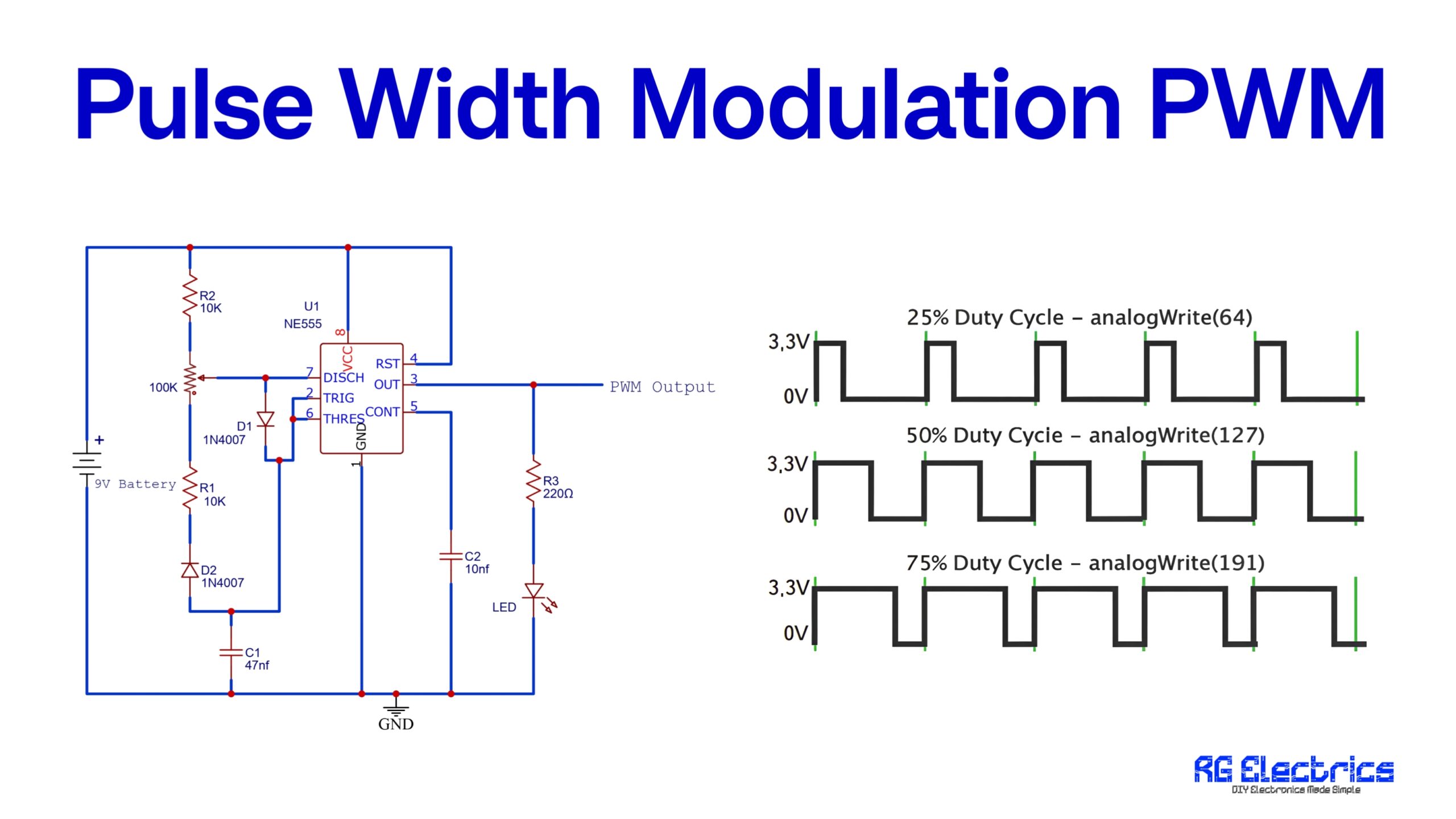
Circuit Diagram

This circuit is a Pulse Width Modulation (PWM) generator using the popular NE555 timer IC in astable mode. Let’s break it down step by step:
1. Power Supply
- The circuit is powered by a 9V battery.
- Pin 8 (VCC) of the NE555 is connected to +9V, and Pin 1 (GND) is grounded.
2. Timing Components
- R1 (10kΩ), R2 (10kΩ), variable resistor (100kΩ pot), D1, D2, and C1 (47nF) form the timing network.
- The resistors and diodes control the charging and discharging paths of capacitor C1.
- By adjusting the potentiometer, the duty cycle (ON/OFF ratio) of the PWM signal changes.
3. Operation of the 555 Timer
- Pins 2 (Trigger) and 6 (Threshold) are connected together and to the timing capacitor C1.
- Pin 7 (Discharge) provides a discharge path for C1.
- Pin 3 (Output) gives the PWM waveform.
4. Diodes Role (D1, D2)
- D1 (1N4007) controls the charging path of C1 through R1 and the potentiometer.
- D2 (1N4007) controls the discharging path through the potentiometer only.
- This separation allows independent control of charge and discharge times, which changes the duty cycle of the PWM signal.
5. Output Stage
- The output at Pin 3 provides the PWM signal.
- An LED with current-limiting resistor (R3, 220Ω) is connected to indicate the PWM effect (LED brightness varies with duty cycle).
- C2 (10nF) at Pin 5 is used for noise filtering and stability.
👉 In short:
- Frequency depends on R1, R2, and C1.
- Duty cycle (PWM control) is adjusted by the 100kΩ potentiometer.
- The circuit generates a PWM signal suitable for controlling devices like motors, LEDs, or other loads.
Applications
- Motor Speed Control
- LED Dimming Control
- Switching Power Supplies
- Audio Signal Generation
- Communication Systems
- Voltage Regulation
- Robotics and Automation
- Inverters and UPS Systems
- Heating Element Control
- Servo Motor Control