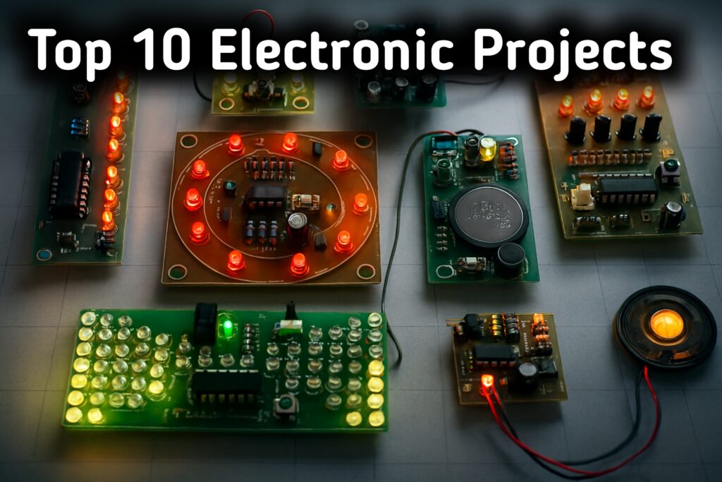
Table of Contents
Introduction
The Schottky diode, also known as the Schottky barrier diode or hot-carrier diode, is a semiconductor device characterized by its low forward voltage drop and fast switching capabilities. It is widely used in power electronics, high-frequency circuits, and protection applications. The unique construction of Schottky diodes makes them highly efficient and suitable for applications where speed and efficiency are crucial.
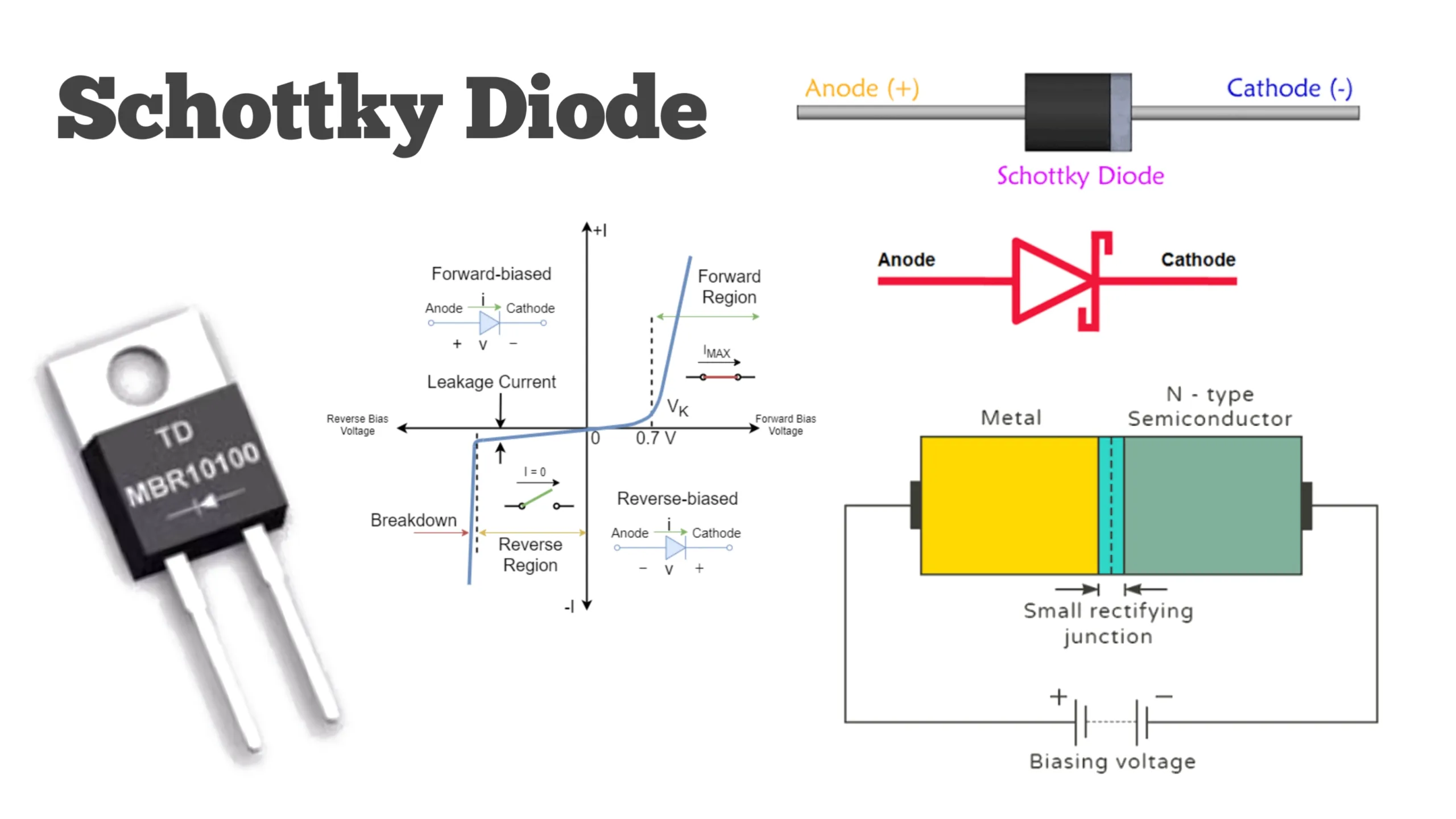
Schottky Diode Symbol
The Schottky diode symbol resembles a standard PN junction diode but with slight modifications to indicate the metal-semiconductor junction. The cathode side of the symbol features a curved line or a distinct variation from the traditional diode symbol, representing the absence of a PN junction and the presence of a Schottky barrier.
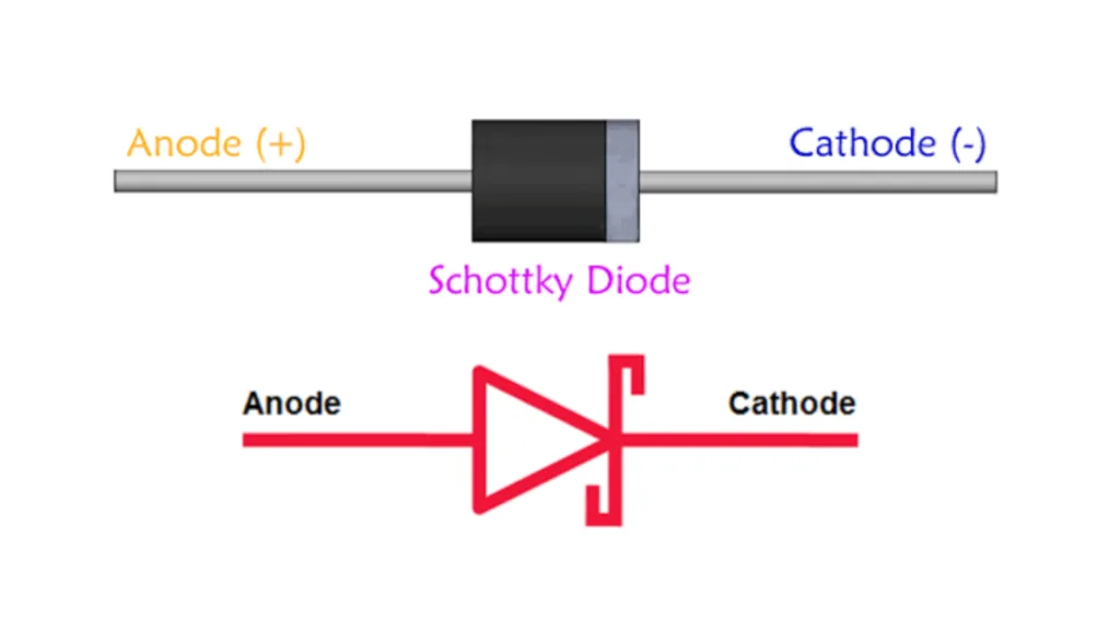
Construction of Schottky Diode
Unlike conventional diodes, which use a PN junction, Schottky diodes use a metal-semiconductor junction to form their rectifying behavior. The key components of a Schottky diode include:
- Metal Contact (Anode): The anode is typically made from metals such as platinum, molybdenum, titanium, or tungsten. The choice of metal determines the diode’s barrier height and electrical properties.
- N-type Semiconductor (Cathode): Silicon, gallium arsenide (GaAs), or silicon carbide (SiC) are commonly used as the semiconductor material.
- Schottky Barrier: The interface between the metal and semiconductor forms the Schottky barrier, controlling the charge carrier movement and defining the diode’s electrical characteristics.
- Thin Depletion Region: Unlike conventional diodes, Schottky diodes have a minimal depletion region, enabling faster switching speeds and lower power losses.
Working Principle of Schottky Diode
The operation of a Schottky diode is primarily governed by the movement of charge carriers across the metal-semiconductor junction.
1. Forward Bias Operation
- When a forward voltage is applied, the barrier potential decreases, allowing electrons from the N-type semiconductor to flow into the metal.
- Since the barrier is lower than in a conventional PN junction diode, conduction occurs at a much lower voltage (~0.2V – 0.3V compared to ~0.7V for silicon PN diodes).
- The result is higher efficiency and lower power dissipation, making Schottky diodes ideal for low-voltage applications.
2. Reverse Bias Operation
- When a reverse voltage is applied, the Schottky barrier increases, restricting the movement of electrons.
- Unlike PN junction diodes, Schottky diodes exhibit higher reverse leakage current due to the absence of a depletion region.
- Excessive reverse voltage can lead to breakdown, which can damage the diode.
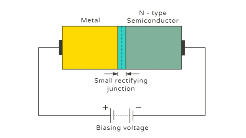
VI Characteristics of Schottky Diode
The voltage-current (VI) characteristics of a Schottky diode are distinct from conventional PN junction diodes due to the metal-semiconductor junction. The key aspects of its VI characteristics are:
1. Forward Bias Characteristics
- The Schottky diode starts conducting at a much lower forward voltage (~0.2V to 0.3V) compared to a PN junction diode (~0.7V).
- The current increases exponentially with voltage in the forward-biased condition.
- Due to its low forward voltage drop, the diode has minimal power dissipation and increased efficiency.
2. Reverse Bias Characteristics
- In the reverse-biased condition, the Schottky barrier prevents current flow.
- However, due to the absence of a depletion region, Schottky diodes exhibit higher reverse leakage current than conventional diodes.
- The diode’s breakdown voltage is lower than that of a PN junction diode, meaning it is not suitable for high-voltage applications.
3. Breakdown Region
- When the reverse voltage applied to the Schottky diode exceeds its breakdown voltage, a sudden increase in reverse current occurs.
- The breakdown voltage of Schottky diodes is typically lower than that of PN junction diodes, making them unsuitable for high-voltage applications.
- Excessive breakdown current can cause thermal runaway and permanent damage to the diode.
- To prevent breakdown, Schottky diodes are often used in low-voltage applications, such as power rectifiers and switching circuits.
Comparison with PN Junction Diode
- Lower Forward Voltage Drop: 0.2V – 0.3V for Schottky diodes vs. 0.7V for silicon PN diodes.
- Higher Reverse Leakage Current: Due to the lack of a depletion layer.
- Faster Switching Speed: No charge storage, making it ideal for high-speed applications.
- Lower Breakdown Voltage: Schottky diodes are limited in high-voltage applications due to early breakdown.
Turn-On and Switching Characteristics
Turn-On Characteristics
- The Schottky diode has an extremely low turn-on voltage (typically 0.2V – 0.3V), which allows it to conduct current at a much lower voltage compared to conventional diodes.
- This property makes it highly efficient for low-power and high-frequency applications.
Switching Characteristics
- The Schottky diode exhibits fast switching speed due to the absence of minority charge carrier storage.
- It has minimal reverse recovery time, making it ideal for high-speed switching circuits.
- The fast response time reduces switching losses, improving efficiency in power electronics applications.
Advantages of Schottky Diodes
- High Efficiency: Reduced forward voltage drop minimizes power loss.
- Fast Response Time: Suitable for high-speed switching applications.
- Minimal Heat Generation: Less power dissipation leads to improved thermal management.
- Ideal for Low Voltage Applications: Widely used in logic circuits and power conversion systems.
Disadvantages of Schottky Diodes
- Higher Reverse Leakage Current: Leads to potential inefficiencies in some applications.
- Limited Breakdown Voltage: Typically lower than PN junction diodes, restricting usage in high-voltage applications.
- Temperature Sensitivity: Performance can be affected by variations in temperature.
Applications of Schottky Diodes
Schottky diodes are extensively used in various electronic and power circuit applications due to their fast switching speed and low voltage drop. Some key applications include:
1. Power Rectification
- Schottky diodes are commonly used in Switch Mode Power Supplies (SMPS) to convert AC to DC efficiently.
- Their low forward voltage drop reduces power dissipation and increases overall system efficiency.
2. High-Frequency Circuits
- Used in RF and microwave applications, including communication systems and radar circuits.
- Their fast switching capabilities make them suitable for frequency multipliers and mixers.
3. Voltage Clamping & Protection Circuits
- Schottky diodes are widely used in clamping circuits to prevent excessive voltage spikes in digital and analog circuits.
- Used in electrostatic discharge (ESD) protection circuits to safeguard sensitive electronic components.
4. Solar Panel Protection
- Schottky diodes are employed in solar photovoltaic systems to prevent reverse current flow, ensuring maximum power extraction from solar panels.
5. Logic Circuits & Digital Applications
- Used in Transistor-Transistor Logic (TTL) circuits to enhance signal processing speed.
- Frequently used in clamping diodes within digital logic gates.
6. Automotive & Aerospace Electronics
- Used in automotive power management systems due to their ability to handle high-speed switching efficiently.
- Used in aerospace applications where efficiency and reliability are critical.
Conclusion
The Schottky diode is a vital component in modern electronics, known for its low forward voltage drop, fast switching speed, and high efficiency. Its unique construction makes it ideal for power rectification, RF applications, voltage clamping, and high-speed logic circuits. Despite its limitations, its benefits make it an indispensable part of numerous electronic systems.