Table of Contents
Introduction:
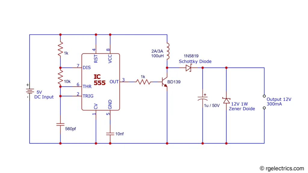
A boost converter is a type of DC-DC converter that steps up a lower input voltage to a higher output voltage. The circuit shown here is a simple 5V to 12V boost converter, designed using the versatile 555 timer IC, an inductor, and a few supporting components. This circuit is ideal for low-power applications where a stable 12V DC output is required, such as powering small electronic devices or modules from a 5V source.
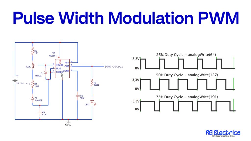
The heart of this boost converter is the 555 timer IC, configured in astable mode to generate a continuous PWM signal. This signal controls the switching of a BD139 transistor, which alternately charges and discharges the inductor. The inductor plays a critical role in storing energy and releasing it at a higher voltage. A Schottky diode and Zener diode ensure efficient and stable operation, while a smoothing capacitor reduces ripples in the output voltage.
This circuit demonstrates the fundamental principles of energy storage and release in inductors, making it a practical and educational project for hobbyists and engineers alike. With a simple design and commonly available components, this boost converter effectively steps up a 5V input to a 12V output, delivering up to 300mA of current.
Component Details:
| S.No | Components | Value | Qty. |
|---|---|---|---|
| 1. | IC | NE555 | 1 |
| 2. | Transistor | BD139 | 1 |
| 3. | Resistor | 1K, 10K | 2, 1 |
| 4. | Capacitor | 1uf/50uF, 560pf, 10nf | 1,1,1 |
| 5. | Diode | 1N5819 | 1 |
| 6. | Zener Diode | 12V 1W | 1 |
| 7. | Inductor | 100uH | 1 |
| 8. | Power Supply | 5V DC | 1 |
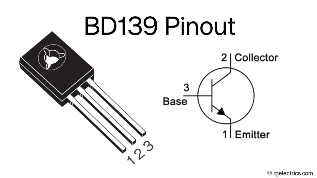
BD139 Pinout:
NE555 Pinout:

Circuit Diagram:
Circuit Explaination:
This circuit is a 5V to 12V boost converter that uses the 555 timer IC in astable mode to generate a high-frequency PWM signal. Here’s how it works:
Components and Their Roles:
- 555 Timer IC:
- Configured in astable mode to produce a continuous square wave signal.
- The frequency and duty cycle are controlled by the 1kΩ and 10kΩ resistors, and the 560pF capacitor.
- Inductor (100µH):
- Stores energy when current flows through it and releases it when the circuit switches off, boosting the voltage.
- BD139 Transistor:
- Acts as a switch controlled by the 555 timer output.
- Alternates between conducting and non-conducting states based on the PWM signal.
- 1N5819 Schottky Diode:
- Prevents reverse current and allows current to flow to the load during the off state of the transistor.
- 1µF Capacitor:
- Smoothens the output by reducing voltage ripples.
- 12V Zener Diode:
- Regulates the output voltage to 12V by clamping it when it exceeds the Zener voltage.
Working:
- The 555 timer generates a high-frequency signal that switches the transistor on and off.
- When the transistor is on, the inductor charges, storing energy as a magnetic field.
- When the transistor switches off, the inductor releases its stored energy, and the combined voltage is boosted.
- The Schottky diode ensures the current flows to the output capacitor and load.
- The Zener diode ensures the output voltage is clamped at 12V.
Output:
- The circuit boosts a 5V DC input to a regulated 12V DC output, capable of delivering up to 300mA.
Applications:
- Microcontroller-Based Projects
- Battery-Powered Devices
- LED Lighting
- Communication Modules
- Small Electronic Gadgets
- Charging Applications
- Testing and Prototyping
- Powering Sensors


