The BD139 is an NPN power transistor designed for medium power linear and switching applications. It is commonly used in audio amplifiers, voltage regulators, and driver circuits. The transistor offers high current gain and can handle relatively large collector currents, making it suitable for use as a driver stage for power transistors. Its compact TO-126 package provides good heat dissipation, allowing it to operate efficiently even under moderate loads.
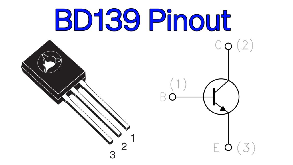
BD139 Pinout Configuration
Pin No.
Pin Name
Description
1
Base (B)
Controls the transistor’s operation; current applied here controls the collector current.
2
Collector (C)
Current flows through this terminal; connected to the load.
3
Emitter (E)
Current leaves through this terminal; usually connected to ground.
Pinout View: When looking at the flat side of the transistor with leads downward, the pin order is Base – Collector – Emitter (B–C–E) from left to right.