Audio amplifiers are an essential part of any sound system, designed to amplify weak audio signals to levels powerful enough to drive speakers. Among the many amplifier designs available, the 100W audio amplifier circuit stands out for its simplicity, efficiency, and reliability, making it an excellent choice for both hobbyists and professional applications. This amplifier is capable of delivering up to 100 watts of output power, suitable for medium to large audio systems, ensuring crystal-clear sound reproduction.
The circuit utilizes a combination of low-power transistors, medium-power drivers, and high-power output transistors for optimal signal amplification and current handling. It is powered by a dual symmetrical power supply, which provides a clean and stable voltage for efficient operation. Designed with a focus on stability and thermal protection, the circuit incorporates feedback and biasing mechanisms to minimize distortion and maintain consistent performance. This article explores the working principles and components of this versatile amplifier design.
Components List
Component Type
Value/Part Number
Quantity
Description
Resistors
100kΩ
1
Input impedance setting
33kΩ
2
Biasing and feedback resistors
4.7kΩ
1
Base resistor
2.2kΩ
1
Biasing resistor
560Ω
2
Differential stage resistors
1kΩ
1
Differential bias resistor
100Ω
2
Feedback and stabilization
33Ω (2W)
2
Driver stage resistor
0.5Ω (5W)
2
Output transistor emitter resistor
Capacitors
10µF (Electrolytic)
3
Coupling and feedback capacitors
100nF (Ceramic)
2
Noise filtering
Transistors
2SA933 (PNP)
4
Differential amplifier stage
2SA945 (PNP)
1
Bias transistor
BD139 (NPN)
1
Driver transistor
BD140 (PNP)
1
Driver transistor
TIP3055 (NPN)
1
Output transistor
TIP2955 (PNP)
1
Output transistor
Diodes
1N4148
4
Thermal stability and biasing
Other Components
Speaker (8Ω, 100W)
1
Output load (speaker)
Power Supply (+35V/-35V)
1
Dual symmetrical power supply
Input Audio Source
1
Input terminal for audio signal
Tip3055 Pinout
Pin Number
Pin Name
1
Base (B)
2
Collector (C)
3
Emitter (E)
TIP2955 Pinout
Pin Number
Pin Name
1
Base (B)
2
Collector (C)
3
Emitter (E)
BD139 Pinout
Pin Number
Pin Name
1
Base (B)
2
Collector (C)
3
Emitter (E)
BD140 Pinout
Pin Number
Pin Name
1
Base (B)
2
Collector (C)
3
Emitter (E)
Circuit Diagram
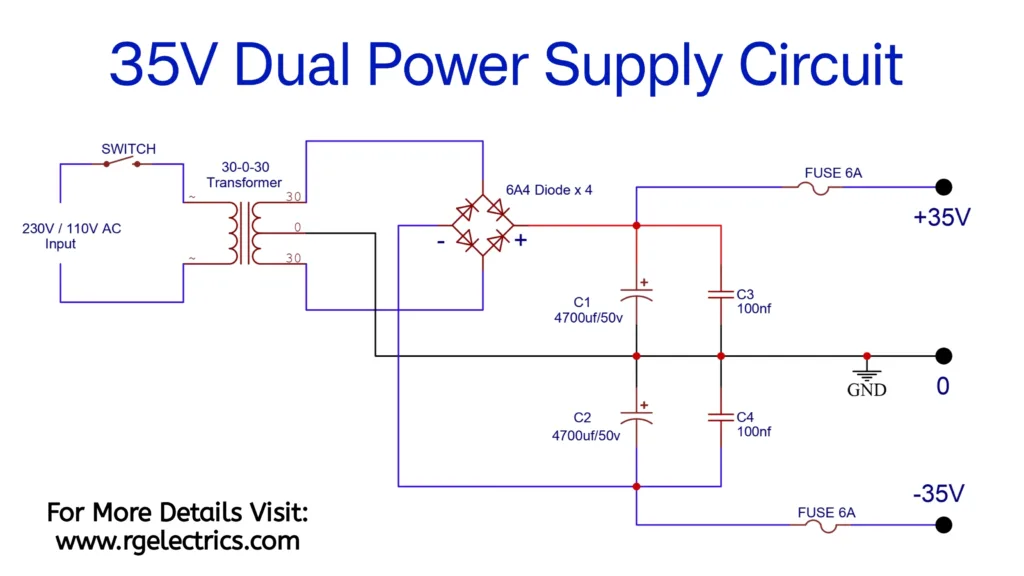
Power Supply Circuit Diagram
Breakdown of its Main Sections and Components:
1. Input Stage
Purpose: This stage takes the audio signal from an external source and prepares it for amplification.
Working:
The input signal is fed through a 10µF capacitor, which blocks any DC component and allows only the AC audio signal to pass.
Resistors (100kΩ and 33kΩ) set the input impedance and ensure the circuit is compatible with most audio sources.
The signal then reaches the differential amplifier stage.
2. Differential Amplifier Stage
Purpose: Provides initial amplification of the input signal while maintaining stability.
Working:
The 2SA933 transistors form a differential pair. These transistors amplify the small input signal, improving its amplitude.
Resistors (560Ω, 33kΩ, and 1kΩ) and capacitors (10µF) set the gain and provide stability to the stage.
The output of this stage is passed to the next driver stage.
3. Driver Stage
Purpose: Prepares the signal for high-power output transistors.
Working:
Transistors BD139 (NPN) and BD140 (PNP) amplify the signal further, providing sufficient drive current for the output stage.
Resistors (4.7kΩ, 33Ω) and diodes (1N4148) ensure proper biasing and thermal compensation for stable operation.
Capacitors (100nF) help filter high-frequency noise, ensuring clean amplification.
4. Output Stage
Purpose: Delivers high power to the speaker, enabling the circuit to drive loads like speakers.
Working:
Power transistors TIP3055 (NPN) and TIP2955 (PNP) handle the large current required to drive the speaker.
Resistors (0.5Ω, 5W) connected in the emitter paths ensure equal current sharing between the transistors and prevent thermal runaway.
This stage amplifies the signal to a level sufficient to drive a speaker up to 100 watts.
5. Feedback Network
Purpose: Provides stability and minimizes distortion.
Working:
A portion of the output signal is fed back to the input stage via a feedback loop consisting of a 100Ω resistor and a 10µF capacitor.
This negative feedback reduces distortion and stabilizes the amplifier’s gain.
6. Power Supply
Purpose: Provides the necessary voltage and current for the circuit.
Working:
The circuit is powered by a dual symmetrical power supply (+35V, -35V).
This ensures a high dynamic range and headroom for amplifying both the positive and negative halves of the input signal without distortion.
7. Output
Purpose: Drives the speaker to produce amplified sound.
Working:
The final amplified signal is passed to the speaker through the SPK terminal.
The speaker reproduces the input audio signal at a higher power level, providing clear and loud sound.
Summary
The circuit efficiently amplifies an input audio signal, maintaining stability and minimizing distortion through its carefully designed stages. The differential amplifier ensures clean amplification, the driver stage boosts the signal further, and the output stage delivers high power to the speaker. Negative feedback enhances performance, while the symmetrical power supply ensures smooth operation across all stages.
You’re welcome! The driver stage in transistor amplifiers plays a crucial role in preparing the signal for the output stage. Here’s more information:
Driver Stage in Transistor Amplifiers
The driver stage is typically the intermediate stage between the small-signal amplification (input stage) and the power amplification (output stage). Its main responsibilities include:
Signal Amplification: It further amplifies the voltage or current from the input stage to levels suitable for driving the output transistors.
Impedance Matching: Ensures proper matching between the input stage and the low-impedance output stage to prevent signal loss.
Current Drive Capability: Provides sufficient base current to the output transistors, which often require significant current to operate effectively, especially in high-power amplifiers.
Stability: Improves circuit stability by minimizing oscillations and ensuring linear operation.
Thermal Protection: Often incorporates biasing diodes or resistors to protect against thermal runaway in the output stage.
Common Configurations Darlington Pair: Two transistors are combined for high current gain and increased drive capability. Complementary Pair: A pair of NPN and PNP transistors are used to ensure symmetrical operation for both positive and negative signal swings.


Thanks for the enlightenment. Kindly shed more information on driver stages of transitior amplifiers.
You’re welcome! The driver stage in transistor amplifiers plays a crucial role in preparing the signal for the output stage. Here’s more information:
Driver Stage in Transistor Amplifiers
The driver stage is typically the intermediate stage between the small-signal amplification (input stage) and the power amplification (output stage). Its main responsibilities include:
Signal Amplification: It further amplifies the voltage or current from the input stage to levels suitable for driving the output transistors.
Impedance Matching: Ensures proper matching between the input stage and the low-impedance output stage to prevent signal loss.
Current Drive Capability: Provides sufficient base current to the output transistors, which often require significant current to operate effectively, especially in high-power amplifiers.
Stability: Improves circuit stability by minimizing oscillations and ensuring linear operation.
Thermal Protection: Often incorporates biasing diodes or resistors to protect against thermal runaway in the output stage.
Common Configurations
Darlington Pair: Two transistors are combined for high current gain and increased drive capability.
Complementary Pair: A pair of NPN and PNP transistors are used to ensure symmetrical operation for both positive and negative signal swings.